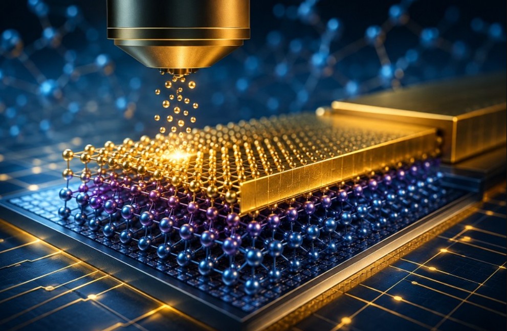
Researchers have developed a new method to grow highly ordered metal films directly onto semiconductors – which could remove one of the biggest barriers to making smaller and more energy-efficient electronic devices.
Modern electronics rely on three basic types of materials: metals, semiconductors, and insulators.
Read the Health Manager: Simple steps can protect painful knees
For years, researchers attempting to improve transistors have focused primarily on the quality of semiconductor materials. The structure of the metals used to make electrical contacts has received far less attention.
That’s starting to become a problem as transistors shrink to the nanoscale. Small structural flaws and disorder inside metals – and especially where metals meet semiconductors – can make it harder for electrical charges to move into and through a device. This creates electrical resistance that can degrade performance and waste energy.
New method: Step-Eva
Researchers led by Chu Junhao at the Shanghai Institute of Technical Physics, part of the Chinese Academy of Sciences, have now developed a technique to overcome this problem.
Their findings were published in Science on August 27.
The new method, called Step-Eva, uses a step-by-step evaporation process to grow highly orderly, single-crystal metal films directly onto semiconductor surfaces.
Traditional metal evaporation usually emits material continuously. Instead, Step-Eva emits an extremely small amount of metal – and then stops. During this waiting period, the newly deposited atoms are given time to move around and settle into more organized positions before a new layer is added.
By repeating this deposition and pause cycle, the formation of small, disordered crystal regions is prevented. Instead, the atoms can gradually join together into larger, highly ordered structures. The result is a single-crystal-metal film with far greater structural uniformity.
Works with multiple metals
The researchers showed that the method works with several metals that are commonly used or studied in electronics, including bismuth, silver, indium, gold, and palladium.
Importantly, these highly ordered metals also created cleaner connections with semiconductor materials. The interfaces suffered less damage and showed fewer local variations in electrical properties. This helped electrical charges move more easily between metal and semiconductor.
When the researchers used the single-crystal metals as contacts for two-dimensional semiconductor transistors, they achieved extremely low contact resistance. N-type transistors reached contact resistance as low as 36 ohm micrometers, while P-type devices reached 145 ohm micrometers.
The transistors also showed on/off current ratios of over 10 billion to one. Even when the channels were reduced to just 50 nanometers, the devices produced on-currents over 1.1 milliamperes per micrometer.
Stable and conductive – even in thin layers
The single-crystal metals also offered other advantages. They remained electrically conductive even when made extremely thin – and showed improved stability at higher temperatures.
The findings suggest that improving metals could become just as important as improving semiconductors, as electronics continue to shrink. By creating cleaner interfaces and allowing electrical charges to flow more efficiently, Step-Eva can provide a new material platform for smaller, faster, and more energy-efficient electronic and optoelectronic devices.
Read on TimePeopleWorld: “If I Go Will They Miss Me”: A Powerful New Voice in 2026 Cinema